Interview with SEM photographer and filmmaker STEFAN DILLER
Cuxhaven, 28.04.2021 – One of the world’s foremost scientific photographers and filmmakers is a pioneering, visionary spaceman who boldly explores the microcosmos. A professional since 1982, Stefan Diller began working with electron microscopes in 1984. What began as a hobby soon evolved into something far beyond professional and artistic work.
“SEM stands for Scanning Electron Microscope. SEM combines all aspects of science I love. Biology, physics, electronics, technology and all this finally culminates into insights into the weaving patterns of nature”, he said.
Dillers’ fascination for small worlds started already during school. “I still recall taking the first glance through my own electron microscope in 1984, an old obsolete Transmission Electron Microscope (TEM) I got from the Free University of Berlin. What I saw was unforgettable. It opened my eyes to an entire new universe of aesthetic structures, absolutely awesome to behold”, Diller continued.
Repairing and sharing the view
To let more people; especially young folks, to experience similar moments of wonder, Diller would later support high schools in setting up electron microscopes that could add hands-on experience into the physics, chemistry, and biology curriculums. “Since the early beginnings, I have had the pleasure to test and work with more than fifty electron microscopes of various brands to date, some of which I repaired, either for my own use or for donating them onwards to high schools.”
The man’s reputation is not only based on scientific projects. It grew and kept on growing further because he managed to open the area of science to public interests and make the mainstreamers stop and look in awe. Coloring the already stunning black and white SEM images adds to the fascinating details and never-before-seen structures of the cosmos all around and inside ourselves. No wonder the wonderful worlds of Stefan Diller also made it into various media and art print outlets. And it did not stop there.
Passion and patience – and the art of Dillers’ NANOFLIGHT®movies
SEM is usually about single images, or a series of images shot from various angles, especially in materials science and nano inspections. A still world, since also specimens like insects or air borne pollutants look like monumental statues. “But what if we could go around them and see them three dimensionally?”
When trying to record a lot of different views of a single specimen in one go, and then compiling the images together, Diller got the idea of his “Nanoflight” movies.
Thus, the photographing artist started and developed yet another career track with his own nanoflight® creator software. “It is an integrated hardware and software solution for a video experience as if flying around a sample within the vacuum chamber”, Diller explained. It took more than three years and the help of many people to develop. Nanoflight® combines the methodology of acquiring colored images with a virtual camera-path in moving the specimen on a nanometer-precise, custom-built piezo-stage in eight degrees of freedom around the specimen.
Although his nano-flights films being undoubtedly awesome, they are also regrettably nano-short. “It takes a full day, 24 hours, to create just one minute, 60 seconds, of video from 1500 SEM-images at 25 frames/second. And each SEM-image requires 50 seconds of beam-time under the electron microscope.”
In the style of “Goldfinger”
Despite the ever-improving SEM technology, there are still limitations, although the development of newer, faster detectors will further reduce the beam time. It still takes many hours. On top of that, prolonged exposures to the electron beam can cause specimen deterioration due to damages or contaminations and warp its appearance. “You can’t work with a light-stand as in normal movies”, Diller said smilingly. Any specimen needs to be elaborately prepared, dehumidified completely and then metal coated or “sputtered”, usually with a very thin layer of gold or platinum, to give it a conducting surface that interacts with the beams emitted. A bit like the full-body gold-cover in “Goldfinger”!
With his own software and state-of-the-art electron microscopes, Diller has made some brilliant movies of structures from the natural world and in the area of material sciences. “Every object I worked with was the most interesting for me at the time because every single one delivered unseen structures and beauty”, Diller recalled.
Showing new eras of medical treatment
Diller also “portrayed” a gene-modified T-cell that was developed to fight lymphoblastic cancer. This was the first gene therapy approved by the US Food and Drug Administration (FDA) in August 2017 and ushered in a new era of medical treatment. “This project was therefore special among all my other special projects. It was really exciting to be part of that historic process and learn about this astonishing new technology,’ he said.
Invited by Google
So much inventive prowess does not go unnoticed: In 2014 he was invited by none other than Google to attend « SciFoo », a series of interdisciplinary scientific conferences around emerging technologies at the renowned Science FOO Camp held by Google Headquarters in Mountainview, California.
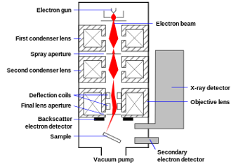
How SEM works (text for schematic SEM image)
The electrons coming back from the surface of an object are recorded, their black and white signal coming from different detectors (which look at the specimen from different sides) are finally converted into different colors, and then recombined to a coloured image.

External links:
For a schematic image: https://en.wikipedia.org/wiki/Scanning_electron_microscope
(German) https://www.lichtmikroskop.net/elektronenmikroskop/rem-mikroskopie.php

